2019-07-08
Foreword
The S parameter is the basic knowledge necessary for engineers in the SI and RF fields. It is easy to find the S, Y, and Z parameters from the network or books. I also wrote the S parameter -- the basics many years ago. But even so, people who have been rolling in the relevant field for many years may still be troubled by some problems. Do you understand the S parameter? Please continue to look down...

1. the difference between individual parameters and serial S parameters
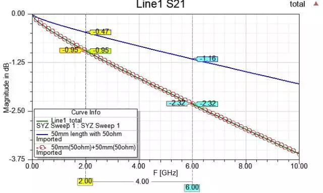
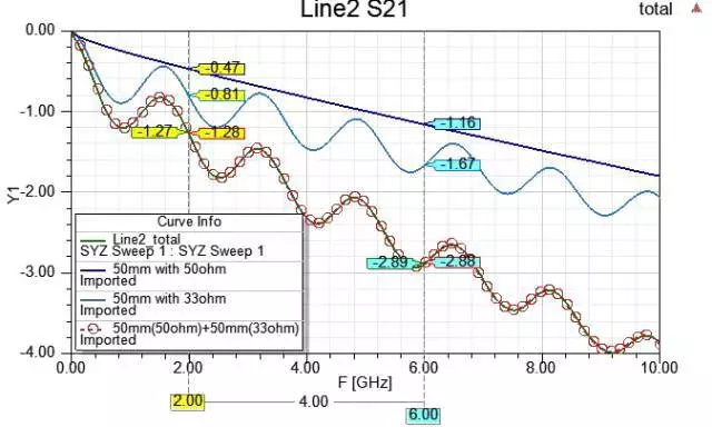
Question 1: Why do you sometimes encounter the S-parameters of each segment, but it is still good, but the string is very poor (loss is not 1+1=2 trend)?
Quick answer : If the real port Zo of each line segment is matched, the loss will be an additive trend, but if the real port Zo of each line segment is very different, then you will see that loss is not cumulative. The trend is because there is more added reflection loss on the tandem junction.
Three transmission lines as shown below
Line2 is also a 100mm long microstrip line. The left 50mm maintains a characteristic impedance of 50 ohms, but the right 50mm line width is doubled and the characteristic impedance is reduced to 33.
Line3 is also a 100mm long microstrip line. The left 50mm maintains a characteristic impedance of 50 ohms, but the right 50mm line width is doubled, the characteristic impedance is reduced to 33, and it is 135o.
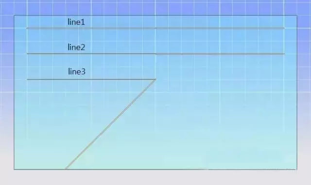
Observing the S21 of Line1, the S parameters of the left and right sections have additive characteristics.
Observing Line2, Line3's S21 found that the S-parameter of the whole line is worse than the S-parameters of the two left and right segments.
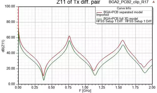
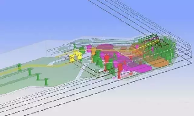
Question 2: Why do I draw the S-parameters of the BGA and the PCB separately and look at the total loss in the Designer, which is different from the result of directly drawing the BGA+PCB to see the S-parameters?
Quick answer : This has an interaction with the structure in 3D space, and the lower port position sometimes has an effect.
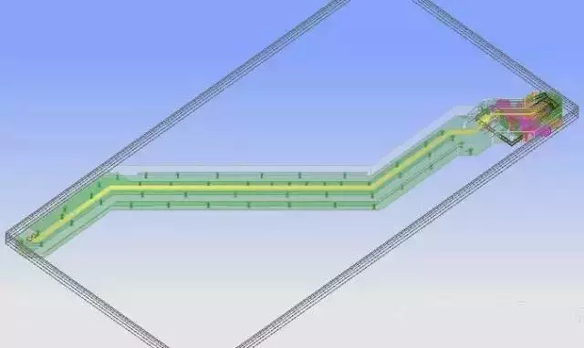
The figure below shows a two-layer BGA package with a two-layer PCB with a complete reference plane, which is a very common application in consumer electronics.
Yellow is a high-speed differential pair signal. The part of the trace on the PCB has a good complete reference plane, but there is no reference plane at the BGA end.
1:the treatment of the double loop S parameter to the ground loop effect
Problem 1: The RLC equivalent circuit can estimate the RLC characteristics of each segment of the signal line and the ground loop, but the S parameter does not work. What is the reason? Does the S parameter have the parasitic effect of the ground loop?
Question 2: When Designer imports the S-parameter model, you can choose whether the circuit symbol of the S-parameter has a reference ground (negative terminal) for each port, or use common ground, and use common ground to indicate whether each port is Is the negative terminal shorted, will the parasitic effect of the ground loop be ignored?
The S parameter itself already contains the effect of the ground loop.
Second, two 2-port can form a 4-port
Is it possible to form a 4-port S parameter with two 2-port S parameters?
Quick answer : No. A 2-port S parameter with 2x2 (4) matrix elements, ie S11, S12, S21, S22, and a 4-port S parameter, which requires a 4x4 (16) matrix unit. So obviously, when there are two 2-port S parameters of two lines, it is not enough to fully and uniquely define a 4-port S parameter, that is, the two-between coupling and the remote coupling condition are not Is defined. In other words, a 4-port S parameter can reduce the two 2-port S parameters by reducing order, but not vice versa.
4.the difference between the S-parameters of the 3D model
The difference between the S parameter of the full 3D model and the S parameter of the separate 3D model
The common problem is: after the S-parameter is separately extracted from the PCB and the PCB, and then the S-parameter is connected in series with the circuit simulation software. What is the difference between the package and the PCB directly in the simulation software?
Quick answer : The spatial coupling path between the package and the PCB on the Z axis will only be considered when the package and the PCB are directly attached to the simulation software in 3D. This is of course the most accurate approach, but it does not need to be done in every case. It depends on the structure and bandwidth considerations. When the coupling effect of this path is affected, under the structure you design, when the influence above a certain bandwidth cannot be ignored, it must be considered.
5.Port impedance setting
The setting of the Port impedance has no effect on the S parameter in essence and the use of the S parameter.
Quick answer : Although renormalize different port impedance, different S-parameter curves are obtained, but the physical effects defined by the N-port model are essentially the same. So the use of model has no effect in theory, but in fact, because of the different value of the tool's transient analysis, the fitting ability sometimes has an effect.
For example, in the early days of SIwave v4.0, it is recommended that the port impedance of the signal be set to 50 ohms, and the port impedance of the power supply should be 0.1~1 ohm, but the current SIwave does not need to do this, that is, you can continue before The setting habits, or all renormalize 50 ohms, SIwave spit out the S parameters to the Designer to use, can get the same result. If you are using other tools that have different port impedance and different time domain simulation results, we recommend you try SIwave.
6.Export S parameter model
When exporting the S parameter model, is there any port renormalize to 50 ohm, which has no effect on the use of S parameters?
Quick answer : No
7.questions and discussions
(1) What should I do if the S parameters cannot be imported?
Ans: First check if the tool feeds back any error message, then open the S parameter with a text editor and check if the frequency description defines the frequency monotonicity. This kind of mistake will occur, usually caused by someone manually editing to modify the S parameter.
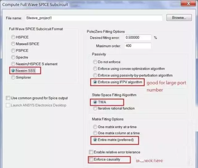
(2) S parameter What should I do if the simulation takes time due to too many ports?
Ans: When I encounter the S-parameter simulation time-consuming, I will first check whether the S-parameter has a passivity and a causality issue, or during the Designer simulation, pay attention to see if it is in the state-space fitting process card for a long time. If you encounter multiple S parameters, try to convert to state space model (.sss), the simulation speed will be much faster, and through SIwave or NdE to state space model, it is recommended to only enforce passivity, no enforce Causality, this will save a lot of time. (Because the state space algorithm itself satisfies the primitive causality, so don't worry about its causality)
(3) What is the main difference between Toushstone 1.0 (TS1.0) and TS2.0?
Ans: TS2.0 (.ts) supports mixed reference impedance, and the reference impedance of each port of TS1.0 (.snp) is the same 50 ohm. Take SIwave as an example:
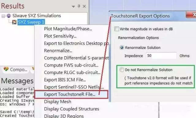
Take NdE (Network Data Explorer) in Designer as an example.
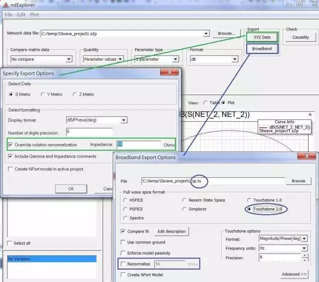
Regardless of whether the original port setting in SIwave or HFSS has specified renormalize, you can decide whether to overwrite renormalize when you finally export.
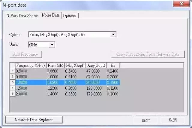
(4) 0Touchstone file can set noise data, what is it, when is it used?
Ans: This is a function defined in TS1.0. You can attach the noise data definition to the Touchstone file, which is generally used for the S-parameter model of the active component.
When you import the S-parameter model in Designer, you can right-click [Edit Model] to view the noise data (if any).
(5) Why, in the example of 2.2, the loss accumulation of the S-parameters of the BGA and the PCB (-0.29-0.8=-1.09) is the difference from the S-parameter (-1.06) obtained by looking at the whole 3D model together?
Ans: When the BGA and the PCB are combined with the 3D to draw the S-parameters, at this time, there is no BGA on the reference plane, and some micro-return path effects contributed by the plane on the PCB through the solder ball will be seen. This can also be verified by observing Z11 (Z profile).