- HOME
- IC PARTNER
- IC Design
- LPC54xxx series

We are pleased to introduce you to our crystal unit
· Items to Confirm (designing of oscillation circuit)
· Selection Guidance for crystal unit
· Crystal Products Lineup
· Oscillation Circuit and Selection Guidance of Crystal Unit.
· Precautions for designing of PCB Board
Please note: to design oscillation circuit, you need to confirm the electronic characteristics as follows:
Oscillation allowance and Negative resistance (-R):
You need to confirm oscillation capability.
We recommend the condition: (-R) / ESR > 5
* -R: Negative resistance, ESR: Equivalent Series Resistance
Drive Level:
You need to confirm if oscillation is stable, and if the drive level is within the specification.
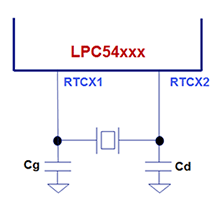
Load Capacitance:
Load capacitance affects frequency stability, oscillation allowance, negative resistance, and start-up time of oscillation.
In addition the load capacitance is determinative factor of crystal unit's load capacitance (CL value) directly.
* frequency stability: frequency deviation out of circuit conditions.
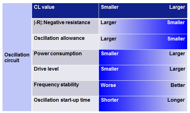
When Customer selects crystal unit, lload capacitance (CL value) is an important factor of the selection.
For instance, crystal with small CL(7.0 pF) makes larger oscillation allowance, smaller current consumption and worse frequency stability,
like below table. Oppositely, crystal with large CL(12.5 pF) makes smaller oscillation allowance, larger current consumption
and better frequency stability.
Please select it in consideration of these characteristics.
|
Product |
Size [mm] |
Applications |
Images |
|
S3215 |
3.2×1.5×0.8t |
Portable equipment |
|
|
Product |
Frequency |
CL*1 |
Product |
External parts *3 |
Drive |
Package |
|
|
Cg |
Cd |
||||||
|
S3215 |
32.768 |
12.5 |
S3215R-32.768K-12.5-20-E |
22 |
18 |
0.008 |
3.2x1.5x0.8 |
|
9.0 |
S3215R-32.768K-9-20-E |
15 |
12 |
0.005 |
|||
|
7.0 |
S3215R-32.768K-7-20-E |
10 |
10 |
0.003 |
|||
|
6.0 |
S3215R-32.768K-6-20-E |
8 |
8 |
0.003 |
|||
Notes:*
1. Load capacitance.
2. Above recommendations are based on actual evaluation results and intended to support users in picking the right components. And the results are only according to the sample set that received from our customers, so it is not including the dispersion trend of IC and the external parts.
As the actual board layout and choice of external components influences the best suitable crystal load capacitance, We do not assume any responsibility and grant warranty for above recommendations. Users design must be verified and decided by own and individual evaluation.
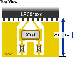
Layout of pins, Crystal unit, Capacitor and Resistor
- Please lay out crystal unit, capacitor and resistor near LPC54xxx as far as possible.
- The length of signal patterns in oscillation circuit should be as short as possible, and do not cross other signal lines.
For 32kHz Crystal Unit
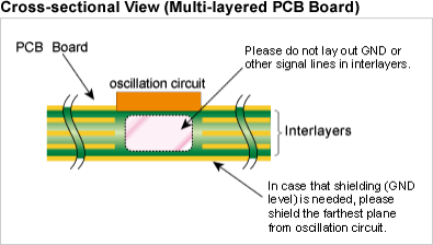
GND Line Pattern and Interconnection of PCB
- Please lay out GND line pattern under crystal unit.
- In case of multi-layered PCB board, do not lay out other signal lines under crystal unit.