2019-07-08
Wafer Level Package (WLCSP) & Flip-Chip
Driven by the small, light and thin drive of electronic products, the packaging field is constantly developing new package types. In the last chapter, it was said that the CSP package is a relatively revolutionary product. Size is 1.2 times or even the same size of the bare chip. Especially with the rise of mobile electronics, this Wafer Level CSP package is the smallest and the smallest. The cost-saving packaging method, although the RDL mask cost is required in the early stage, it saves the cost of the Lead frame, and the direct solder bump can be soldered to the motherboard.
The concept of CSP (Chip-Scale or Chipe-Size Package) originated in 1990s, followed by IPC/JEDEC J-STD-012 standard, which is mainly applied to Low pin count EEPROMs, ASICs and microprocessors (MCU), especially when The bigger the Wafer and the smaller the Die, the more cost advantage.
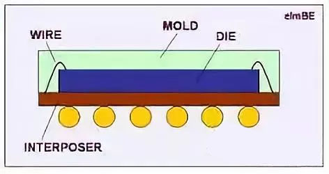
The main steps of the CSP package are: Mount the die on the epoxy interposer, and then connect the PAD to the substrate with a wire bond (gold or Al). The third step is to protect the Die and Wire with the Molding Plastic package, and finally paste the Solder ball. The bottom of Interposer.
Of course, the above wire bond will make the package larger than the die size. Moreover, the wire from the die to the lead frame also has a connection impedance. Later, it was developed to use bump instead of wire bond, so the Flip chip was replaced by the wire bond package, which saved the space of the wire bond, so it can be done. Die almost waited for the size of the package.
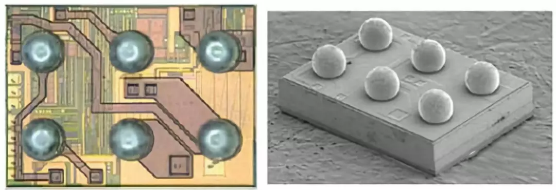
When it comes to Flip-Chip, it's natural to talk about this bump. It's impossible to cut the die and then grow the bump, so you must finish the process before Wafer has cut it. So it is called Wafer Level CSP package (WLCSP).
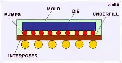
The main three steps of the Flip-Chip package, the long bumps on the Die, the face-down dies of the good ball are attached to the substrate or substrate, and then underfilled.
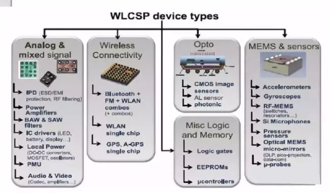
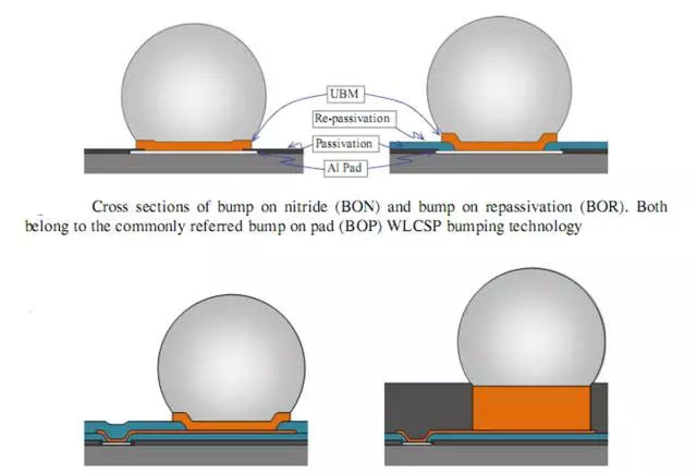
WLCSP is now the mainstream of packaging technology, there are two main types, one is direct BOP (Bump On Pad), and the other is RDL (Redistribution Layer). BOP technology also needs to be re-passivated according to whether it needs Poly, and then divided into BON (Bump on SiN) and BOR (Bump on Repassivation). BOP is widely used in Analog/Power packages. Since the current flows directly vertically, there is no lateral RDL, so it is advantageous for power device packaging, and the cost is low, but its Pin count is limited, so it develops to RDL+. Bump. BOP directly anchors UBM/Bump on Top Metal's PAD, while RDL+Bump is isolated and routed with Polymer (Polyimide or PBO) and separates Bump from the device surface.
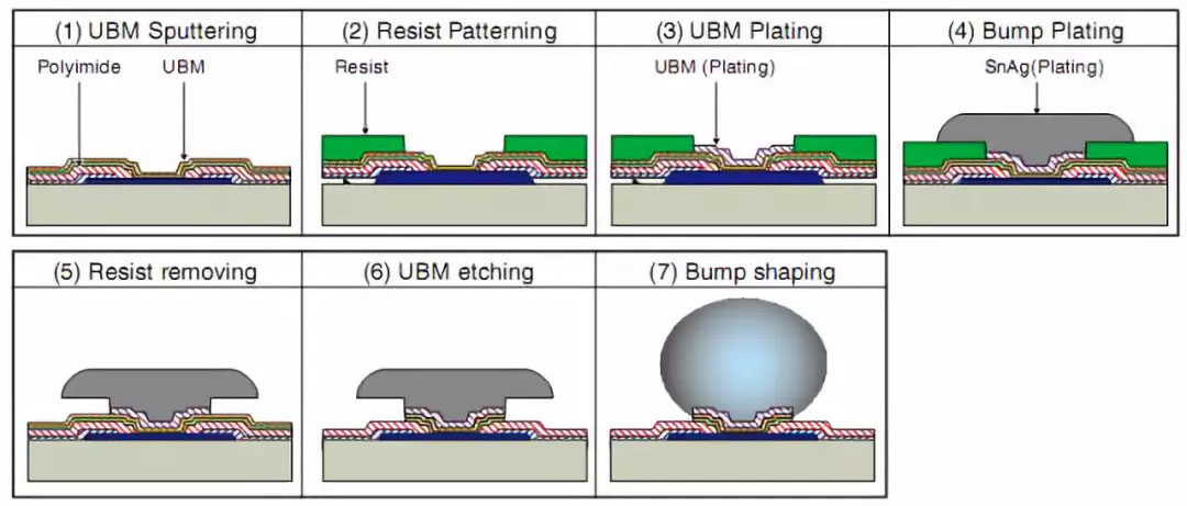
Let's talk about the process flow of RDL+Bump+ copper column. It is similar to the FAB process, and a four-layer mask can be used. The dielectric between RDLs is isolated with Polyimide. Metal can be plated up (Seed uses Sputter).
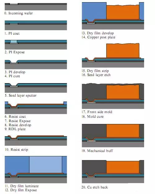
The RDL+Bump after molding is as shown below:
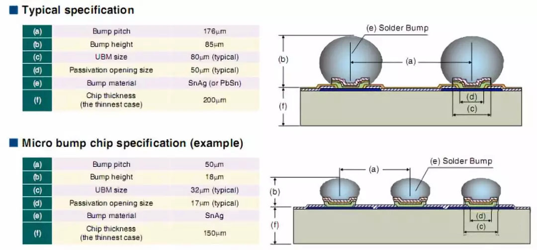
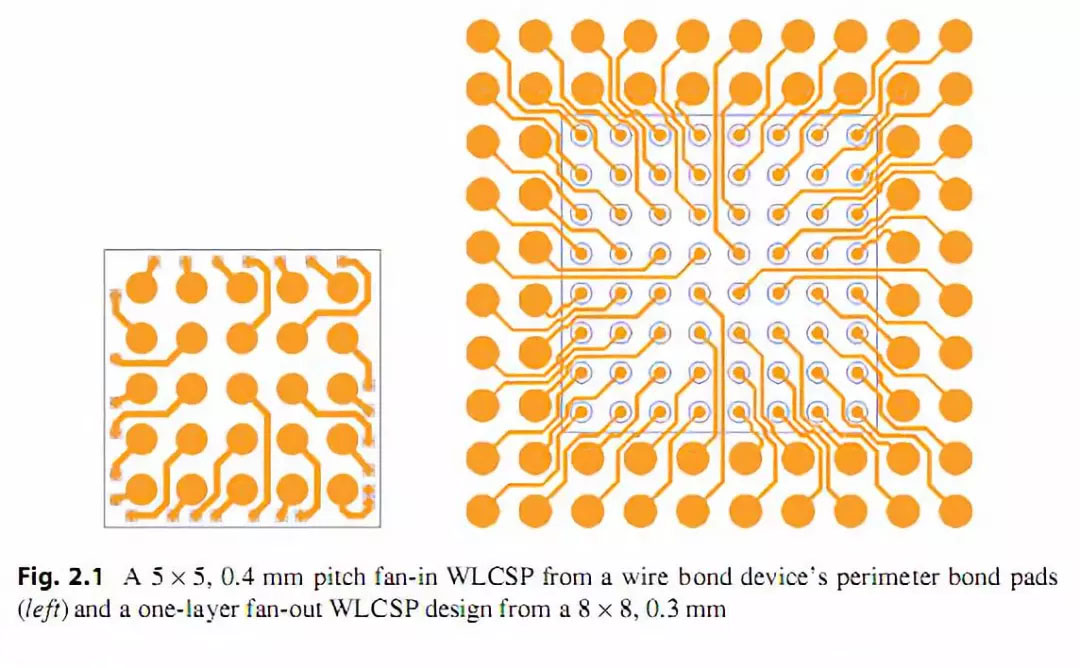
The earliest WLCSP was Fan-In, meaning that all bumps were on the die, and the connection between die and Pad was mainly connected by RDL's Metal Line. Corresponding to this is the Fan-Out WLCSP package, which is to make the bump grow outside the chip (1.2 times), the area is larger, the pressure of the bump will not damage the chip.
Before talking about the solder ball, what is the difference between Flip-Chip and WLCSP? Flip-chip generally still needs a substrate, but it is flipped over by the solder ball (instead of the Wire bond), and the WLCSP is a good ball and is directly attached to the PCB.
Well, whether Flip-Chip or WLCSP needs a thing called Solder Ball, then it's time to explain Solder Ball, how these Bumps grow up.
Let me talk about using a solder ball first? That is to answer a question, what is the technical requirements of Solder Ball?